
Robert W. Dutton – författare
Visar alla böcker från författaren . Handla med fri frakt och snabb leverans.
5 produkter
5 produkter

Del 243 - Springer International Series in Engineering and Computer Science
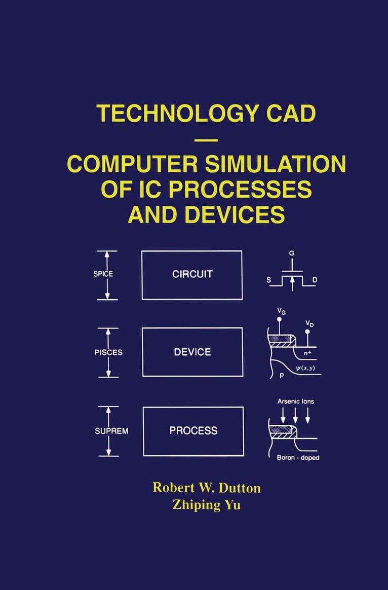
Technology CAD — Computer Simulation of IC Processes and Devices
Inbunden, Engelska, 1993
2 373 kr
Skickas inom 10-15 vardagar
129 3.6 Exercises 130 3.7 References. 131 4 PN Junctions 131 4.1 Introduction. 132 4.2 Carrier Densities: Equilibrium Case 4.3 Non-Equilibrium .......... . 139 4.4 Carrier Transport and Conservation 144 4.5 The pn Junction - Equilibrium Conditions. 147 155 4.6 The pn Junction - Non-equilibrium. 4.7 SEDAN Analysis . . . . . . . . . . . . . 166 4.7.1 Heavy Doping Effects ..... . 176 4.7.2 Analysis of High-Level Injection 181 190 4.7.3 Technology-Dependent Device Effects 4.8 Summary 193 4.9 Exercises 193 194 4.10 References. 5 MOS Structures 197 5.1 Introduction ............. . 197 5.2 The MOS Capacitor ........ . 198 5.3 Basic MOSFET I-V Characteristics. 208 5.4 Threshold Voltage in Nonuniform Substrate 217 5.5 MOS Device Design by Simulation . . . . . 224 5.5.1 Body-bias Sensitivity of Threshold Voltage 225 5.5.2 Two-region Model . . . . . . . . 231 5.5.3 MOSFET Design by Simulation. 234 5.6 Summary 240 5.7 Exercises 240 5.8 References. 242 6 Bipolar Transistors 243 6.1 Introduction ... 243 6.2 Lateral pnp Transistor Operation 245 6.3 Transport Current Analysis ... 252 6.4 Generalized Charge Storage Model 260 6.,1) Transistor Equivalent Circuits. 267 6.5.1 Charge Control Model ...
Del 243 - Springer International Series in Engineering and Computer Science
Technology CAD — Computer Simulation of IC Processes and Devices
Häftad, Engelska, 2012
2 373 kr
Skickas inom 10-15 vardagar
129 3.6 Exercises 130 3.7 References. 131 4 PN Junctions 131 4.1 Introduction. 132 4.2 Carrier Densities: Equilibrium Case 4.3 Non-Equilibrium .......... . 139 4.4 Carrier Transport and Conservation 144 4.5 The pn Junction - Equilibrium Conditions. 147 155 4.6 The pn Junction - Non-equilibrium. 4.7 SEDAN Analysis . . . . . . . . . . . . . 166 4.7.1 Heavy Doping Effects ..... . 176 4.7.2 Analysis of High-Level Injection 181 190 4.7.3 Technology-Dependent Device Effects 4.8 Summary 193 4.9 Exercises 193 194 4.10 References. 5 MOS Structures 197 5.1 Introduction ............. . 197 5.2 The MOS Capacitor ........ . 198 5.3 Basic MOSFET I-V Characteristics. 208 5.4 Threshold Voltage in Nonuniform Substrate 217 5.5 MOS Device Design by Simulation . . . . . 224 5.5.1 Body-bias Sensitivity of Threshold Voltage 225 5.5.2 Two-region Model . . . . . . . . 231 5.5.3 MOSFET Design by Simulation. 234 5.6 Summary 240 5.7 Exercises 240 5.8 References. 242 6 Bipolar Transistors 243 6.1 Introduction ... 243 6.2 Lateral pnp Transistor Operation 245 6.3 Transport Current Analysis ... 252 6.4 Generalized Charge Storage Model 260 6.,1) Transistor Equivalent Circuits. 267 6.5.1 Charge Control Model ...
E-bok
PDF, Engelska, 20123 157 kr
Läs direkt efter köp
129 3.6 Exercises 130 3.7 References. 131 4 PN Junctions 131 4.1 Introduction. 132 4.2 Carrier Densities: Equilibrium Case 4.3 Non-Equilibrium .......... . 139 4.4 Carrier Transport and Conservation 144 4.5 The pn Junction - Equilibrium Conditions. 147 155 4.6 The pn Junction - Non-equilibrium. 4.7 SEDAN Analysis . . . . . . . . . . . . . 166 4.7.1 Heavy Doping Effects ..... . 176 4.7.2 Analysis of High-Level Injection 181 190 4.7.3 Technology-Dependent Device Effects 4.8 Summary 193 4.9 Exercises 193 194 4.10 References. 5 MOS Structures 197 5.1 Introduction ............. . 197 5.2 The MOS Capacitor ........ . 198 5.3 Basic MOSFET I-V Characteristics. 208 5.4 Threshold Voltage in Nonuniform Substrate 217 5.5 MOS Device Design by Simulation . . . . . 224 5.5.1 Body-bias Sensitivity of Threshold Voltage 225 5.5.2 Two-region Model . . . . . . . . 231 5.5.3 MOSFET Design by Simulation. 234 5.6 Summary 240 5.7 Exercises 240 5.8 References. 242 6 Bipolar Transistors 243 6.1 Introduction ... 243 6.2 Lateral pnp Transistor Operation 245 6.3 Transport Current Analysis ... 252 6.4 Generalized Charge Storage Model 260 6.,1) Transistor Equivalent Circuits. 267 6.5.1 Charge Control Model ...
E-bok
PDF, Engelska, 2012712 kr
Läs direkt efter köp
P. Antognetti University of Genova, Italy Director of the NATO ASI The key importance of VLSI circuits is shown by the national efforts in this field taking place in several countries at differ ent levels (government agencies, private industries, defense de partments). As a result of the evolution of IC technology over the past two decades, component complexi ty has increased from one single to over 400,000 transistor functions per chip. Low cost of such single chip systems is only possible by reducing design cost per function and avoiding cost penalties for design errors. Therefore, computer simulation tools, at all levels of the design process, have become an absolute necessity and a cornerstone in the VLSI era, particularly as experimental investigations are very time-consuming, often too expensive and sometimes not at all feasible. As minimum device dimensions shrink, the need to understand the fabrication process in a quanti tati ve way becomes critical. Fine patterns, thin oxide layers, polycristalline silicon interco~ nections, shallow junctions and threshold implants, each become more sensitive to process variations. Each of these technologies changes toward finer structures requires increased understanding of the process physics. In addition, the tighter requirements for process control make it imperative that sensitivities be unde~ stood and that optimation be used to minimize the effect of sta tistical fluctuations.
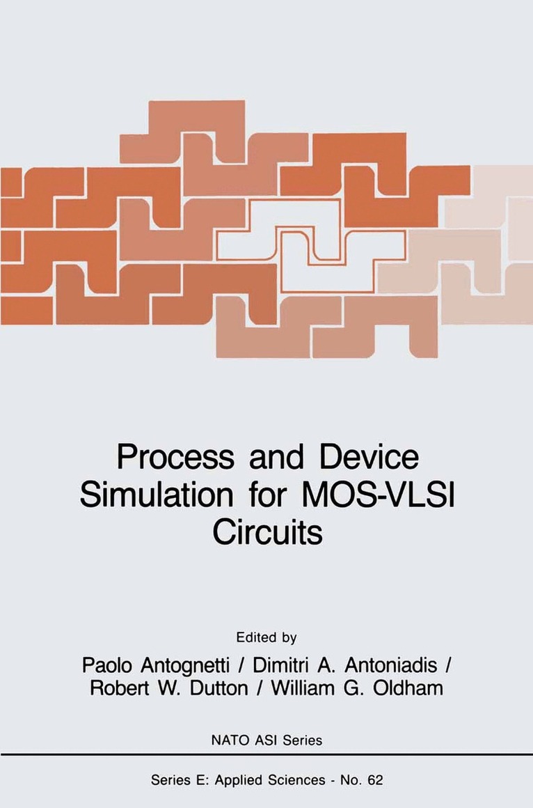
Häftad, Engelska, 2011
545 kr
Skickas inom 10-15 vardagar
P. Antognetti University of Genova, Italy Director of the NATO ASI The key importance of VLSI circuits is shown by the national efforts in this field taking place in several countries at differ ent levels (government agencies, private industries, defense de partments). As a result of the evolution of IC technology over the past two decades, component complexi ty has increased from one single to over 400,000 transistor functions per chip. Low cost of such single chip systems is only possible by reducing design cost per function and avoiding cost penalties for design errors. Therefore, computer simulation tools, at all levels of the design process, have become an absolute necessity and a cornerstone in the VLSI era, particularly as experimental investigations are very time-consuming, often too expensive and sometimes not at all feasible. As minimum device dimensions shrink, the need to understand the fabrication process in a quanti tati ve way becomes critical. Fine patterns, thin oxide layers, polycristalline silicon interco~ nections, shallow junctions and threshold implants, each become more sensitive to process variations. Each of these technologies changes toward finer structures requires increased understanding of the process physics. In addition, the tighter requirements for process control make it imperative that sensitivities be unde~ stood and that optimation be used to minimize the effect of sta tistical fluctuations.