• Fri frakt över 249 kr
  • •
  • Snabba leveranser
  • •
  • Billiga böcker
Kundservice

Du är på sajten för privatpersoner.

Företag, bibliotek eller offentlig verksamhet?

Du handlar på classic.bokus.com, där alla dina funktioner finns intakta.
Till classic.bokus.com
Bokus logotyp. Gå till startsidan.
  • Erbjudanden
  • Student
  • Topplistor
  • Barn & ungdom
  • Bokus Play
  • E-böcker
  • Ljudböcker
  • Pocketböcker
  • Spel och pussel

5% studentrabatt – använd koden KURSBOK27 →

Sidfot

Mina sidor

    Hjälp

    • Kundservice
    • Vanliga frågor och svar
    • Frakt och leverans
    • Retur vid ångerrätt
    • Reklamera vara
    • Betalning
    • Köpvillkor
    • Allmänna villkor
    • Information om webbplatsens tillgänglighet

    Om Bokus

    • Om oss
    • Pressrum
    • För studenter
    • För företag
    • För bibliotek och offentlig verksamhet
    • För leverantörer
    • Hållbarhet

    Populärt

    • Aktuella erbjudanden
    • Presentkort
    • Studentlitteratur
    • Nya böcker
    • Topplistor
    • Signerade böcker
    • Engelska böcker

    Inspiration

    • Boktips
    • BookTok
    • Barnbokskaraktärer
    • Populära författare
    Logotyp för Bokus
    Följ oss på Facebook (extern länk)Följ oss på Instagram (extern länk)Följ oss på YouTube (extern länk)Följ oss på TikTok (extern länk)
    bokus @ CookiesAnpassa cookiesIntegritetspolicyKöpvillkor
    Till Citymail hemsida (extern länk)Till Budbee hemsida (extern länk)Till Postnord hemsida (extern länk)Till Schenker hemsida (extern länk)Till Early Bird hemsida (extern länk)Till Walleys hemsida (extern länk)
    1. Naturvetenskap och teknik
    2. Teknik och industri
    3. Energiteknik

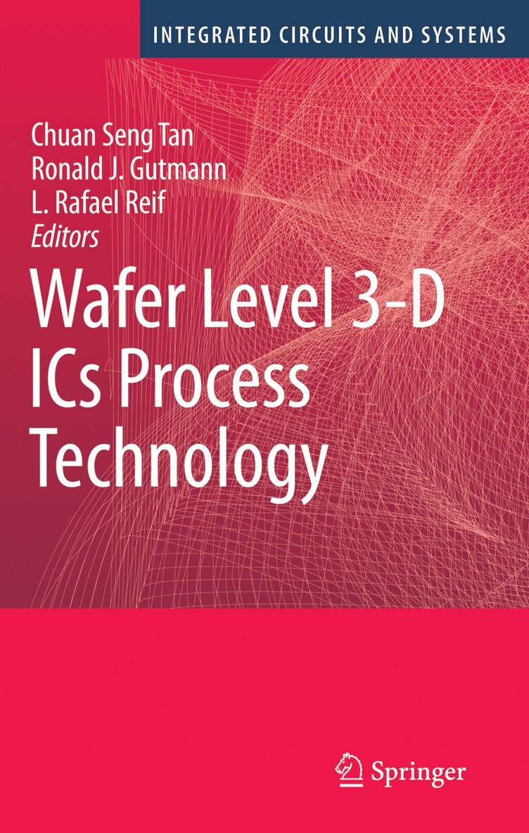
    Wafer Level 3-D ICs Process Technology

    AvChuan Seng Tan,Ronald J. Gutmann

    Inbunden, Engelska, 2008

    Del i serien Integrated Circuits and Systems

    1 614 kr

    Beställningsvara. Skickas inom 10-15 vardagar. Fri frakt över 249 kr.

    Beskrivning

    Three-dimensional (3D) integration is clearly the simplest answer to most of the semiconductor industry’s vexing problems: heterogeneous integration and red- tions of power, form factor, delay, and even cost. Conceptually the power, latency, and form factor of a system with a ?xed number of transistors all scale roughly linearly with the diameter of the smallest sphere enclosing frequently interacting devices. This clearly provides the fundamental motivation behind 3D technologies which vertically stack several strata of device and interconnect layers with high vertical interconnectivity. In addition, the ability to vertically stack strata with - vergent and even incompatible process ?ows provides for low cost and low parasitic integration of diverse technologies such as sensors, energy scavengers, nonvolatile memory, dense memory, fast memory, processors, and RF layers. These capabilities coupled with today’s trends of increasing levels of integrated functionality, lower power, smaller form factor, increasingly divergent process ?ows, and functional diversi?cation would seem to make 3D technologies a natural choice for most of the semiconductor industry. Since the concept of vertical integration of different strata has been around for over 20 years, why aren’t vertically stacked strata endemic to the semiconductor industry? The simple answer to this question is that in the past, the 3D advantages while interesting were not necessary due to the tremendous opportunities offered by geometric scaling. In addition, even when the global interconnect problem of high-performance single-core processors seemed insurmountable without inno- tions such as 3D, alternative architectural solutions such as multicores could eff- tivelydelaybutnoteliminatetheneedfor3D.

    Produktinformation

    • Utgivningsdatum:2008-09-19
    • Mått:155 x 235 x 25 mm
    • Vikt:729 g
    • Format:Inbunden
    • Språk:Engelska
    • Serie:Integrated Circuits and Systems
    • Antal sidor:410
    • Upplaga:2009
    • Förlag:Springer-Verlag New York Inc.
    • ISBN:9780387765327

    Utforska kategorier

    • Energiteknik inom Naturvetenskap och teknik

    Innehållsförteckning

    • Overview of Wafer-Level 3D ICs.- Monolithic 3D Integrated Circuits.- Stacked CMOS Technologies.- Wafer-Bonding Technologies and Strategies for 3D ICs.- Through-Silicon Via Fabrication, Backgrind, and Handle Wafer Technologies.- Cu Wafer Bonding for 3D IC Applications.- Cu/Sn Solid#x2013;Liquid Interdiffusion Bonding.- An SOI-Based 3D Circuit Integration Technology.- 3D Fabrication Options for High-Performance CMOS Technology.- 3D Integration Based upon Dielectric Adhesive Bonding.- Direct Hybrid Bonding.- 3D Memory.- Circuit Architectures for 3D Integration.- Thermal Challenges of 3D ICs.- Status and Outlook.