
Evgeni Gusev – författare
Visar alla böcker från författaren . Handla med fri frakt och snabb leverans.
16 produkter
16 produkter

Inbunden, Engelska, 2006
1 620 kr
Skickas inom 10-15 vardagar
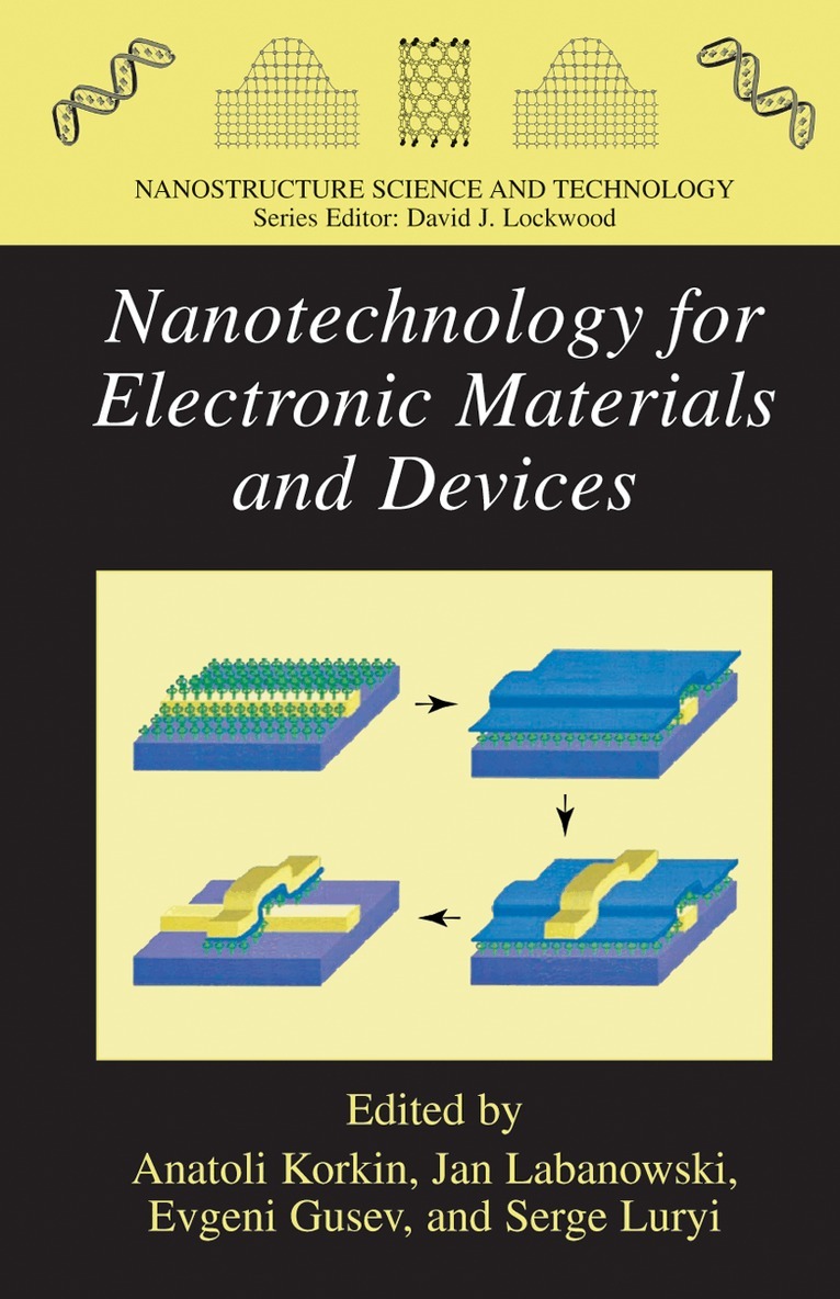
The high level of attention and interest of the global community to NANO science and technology to a large extent is linked to the GIGAntic challenges for the c- tinuing growth of information technology, which sparked an unprecedented level of interdisciplinary and international cooperation among industrial and academic researchers, companies, IT market rivals, and countries, including former political and military rivals . Microelectronics technologies have reached a new stage in their development: The latest miniaturization of electronic devices is approaching atomic dimensions, interconnect bottlenecks are limiting circuit speeds, new ma- rials are being introduced into microelectronics manufacture at an unprecedented rate , and alternative technologies to mainstream complementary metal-oxide sem- conductors (CMOSs) are being considered . The very dynamic stage of science and technology related to the advanced and future electronics and photonics creates a growing gap between the large number of rapid publications and nanotechnology highlights in media on one side and fundamental understanding of underlying phenomena and an adequate evaluation of scientific discoveries and technological innovations on the other side. Writing a tutorial book on fundamentals of science and technology for electronics at this time is almost the same level of challenge as writing a history book during a revolution.
E-bok
PDF, Engelska, 20102 049 kr
Läs direkt efter köp
The high level of attention and interest of the global community to NANO science and technology to a large extent is linked to the GIGAntic challenges for the c- tinuing growth of information technology, which sparked an unprecedented level of interdisciplinary and international cooperation among industrial and academic researchers, companies, IT market rivals, and countries, including former political and military rivals . Microelectronics technologies have reached a new stage in their development: The latest miniaturization of electronic devices is approaching atomic dimensions, interconnect bottlenecks are limiting circuit speeds, new ma- rials are being introduced into microelectronics manufacture at an unprecedented rate , and alternative technologies to mainstream complementary metal-oxide sem- conductors (CMOSs) are being considered . The very dynamic stage of science and technology related to the advanced and future electronics and photonics creates a growing gap between the large number of rapid publications and nanotechnology highlights in media on one side and fundamental understanding of underlying phenomena and an adequate evaluation of scientific discoveries and technological innovations on the other side. Writing a tutorial book on fundamentals of science and technology for electronics at this time is almost the same level of challenge as writing a history book during a revolution.
Inbunden, Engelska, 1998
1 620 kr
Skickas inom 10-15 vardagar
An extrapolation of ULSI scaling trends indicates that minimum feature sizes below 0.1 mu and gate thicknesses of <3 nm will be required in the near future. Given the importance of ultrathin gate dielectrics, well-focused basic scientific research and aggressive development programs must continue on the silicon oxide, oxynitride, and high K materials on silicon systems, especially in the critical, ultrathin 1-3 nm regime. The main thrust of the present book is a review, at the nano and atomic scale, the complex scientific issues related to the use of ultrathin dielectrics in next-generation Si-based devices. The contributing authors are leading scientists, drawn from academic, industrial and government laboratories throughout the world, and representing such backgrounds as basic and applied physics, chemistry, electrical engineering, surface science, and materials science. Audience: Both expert scientists and engineers who wish to keep up with cutting edge research, and new students who wish to learn more about the exciting basic research issues relevant to next-generation device technology.

Häftad, Engelska, 1998
1 620 kr
Skickas inom 10-15 vardagar
An extrapolation of ULSI scaling trends indicates that minimum feature sizes below 0.1 mu and gate thicknesses of <3 nm will be required in the near future. Given the importance of ultrathin gate dielectrics, well-focused basic scientific research and aggressive development programs must continue on the silicon oxide, oxynitride, and high K materials on silicon systems, especially in the critical, ultrathin 1-3 nm regime. The main thrust of the present book is a review, at the nano and atomic scale, the complex scientific issues related to the use of ultrathin dielectrics in next-generation Si-based devices. The contributing authors are leading scientists, drawn from academic, industrial and government laboratories throughout the world, and representing such backgrounds as basic and applied physics, chemistry, electrical engineering, surface science, and materials science. Audience: Both expert scientists and engineers who wish to keep up with cutting edge research, and new students who wish to learn more about the exciting basic research issues relevant to next-generation device technology.
Häftad, Engelska, 2014
384 kr
Skickas inom 7-10 vardagar
Symposium S, 'Microelectromechanical Systems - Materials and Devices IV', held November 29-December 3 at the 2010 MRS Fall Meeting in Boston, Massachusetts, focused on micro- and nanoelectromechanical systems (MEMS/NEMS), technologies which were spawned from the fabrication and integration of small-scale mechanical, electrical, thermal, magnetic, fluidic and optical sensors and actuators with micro-electronic components. MEMS and NEMS have enabled performance enhancements and manufacturing cost reductions in a number of applications, including optical displays, acceleration sensing, radio-frequency switching, drug delivery, chemical detection and power generation and storage. Although originally based on silicon microelectronics, the reach of MEMS and NEMS has extended well beyond traditional engineering materials and now includes nanomaterials (nanotubes, nanowires, nanoparticles), smart materials (piezoelectric and ferroelectric materials, shape memory alloys, pH-sensitive polymers), metamaterials and biomaterials (ceramic, metallic, polymeric, composite-based implant materials). While these new materials provide more freedom with regards to the design space of MEMS and NEMS, they also introduce a number of new fabrication and characterization challenges not previously encountered with silicon-based technology.

Inbunden, Engelska, 2006
2 158 kr
Skickas inom 10-15 vardagar
The goal of this NATO Advanced Research Workshop (ARW) entitled “Defects in Advanced High-k Dielectric Nano-electronic Semiconductor Devices”, which was held in St. Petersburg, Russia, from July 11 to 14, 2005, was to examine the very complex scientific issues that pertain to the use of advanced high dielectric constant (high-k) materials in next generation semiconductor devices. The special feature of this workshop was focus on an important issue of defects in this novel class of materials. One of the key obstacles to high-k integration into Si nano-technology are the electronic defects in high-k materials. It has been established that defects do exist in high-k dielectrics and they play an important role in device operation. However, very little is known about the nature of the defects or about possible techniques to eliminate, or at least minimize them. Given the absence of a feasible alternative in the near future, well-focused scientific research and aggressive development programs on high-k gate dielectrics and related devices must continue for semiconductor electronics to remain a competitive income producing force in the global market.

Häftad, Engelska, 2006
2 158 kr
Skickas inom 10-15 vardagar
The goal of this NATO Advanced Research Workshop (ARW) entitled “Defects in Advanced High-k Dielectric Nano-electronic Semiconductor Devices”, which was held in St. Petersburg, Russia, from July 11 to 14, 2005, was to examine the very complex scientific issues that pertain to the use of advanced high dielectric constant (high-k) materials in next generation semiconductor devices. The special feature of this workshop was focus on an important issue of defects in this novel class of materials. One of the key obstacles to high-k integration into Si nano-technology are the electronic defects in high-k materials. It has been established that defects do exist in high-k dielectrics and they play an important role in device operation. However, very little is known about the nature of the defects or about possible techniques to eliminate, or at least minimize them. Given the absence of a feasible alternative in the near future, well-focused scientific research and aggressive development programs on high-k gate dielectrics and related devices must continue for semiconductor electronics to remain a competitive income producing force in the global market.
E-bok
PDF, Engelska, 20062 840 kr
Läs direkt efter köp
The goal of this NATO Advanced Research Workshop (ARW) entitled “Defects in Advanced High-k Dielectric Nano-electronic Semiconductor Devices”, which was held in St. Petersburg, Russia, from July 11 to 14, 2005, was to examine the very complex scientific issues that pertain to the use of advanced high dielectric constant (high-k) materials in next generation semiconductor devices. The special feature of this workshop was focus on an important issue of defects in this novel class of materials. One of the key obstacles to high-k integration into Si nano-technology are the electronic defects in high-k materials. It has been established that defects do exist in high-k dielectrics and they play an important role in device operation. However, very little is known about the nature of the defects or about possible techniques to eliminate, or at least minimize them. Given the absence of a feasible alternative in the near future, well-focused scientific research and aggressive development programs on high-k gate dielectrics and related devices must continue for semiconductor electronics to remain a competitive income producing force in the global market.
Häftad, Engelska, 2011
1 620 kr
Skickas inom 10-15 vardagar
The high level of attention and interest of the global community to NANO science and technology to a large extent is linked to the GIGAntic challenges for the c- tinuing growth of information technology, which sparked an unprecedented level of interdisciplinary and international cooperation among industrial and academic researchers, companies, IT market rivals, and countries, including former political and military rivals . Microelectronics technologies have reached a new stage in their development: The latest miniaturization of electronic devices is approaching atomic dimensions, interconnect bottlenecks are limiting circuit speeds, new ma- rials are being introduced into microelectronics manufacture at an unprecedented rate , and alternative technologies to mainstream complementary metal-oxide sem- conductors (CMOSs) are being considered . The very dynamic stage of science and technology related to the advanced and future electronics and photonics creates a growing gap between the large number of rapid publications and nanotechnology highlights in media on one side and fundamental understanding of underlying phenomena and an adequate evaluation of scientific discoveries and technological innovations on the other side. Writing a tutorial book on fundamentals of science and technology for electronics at this time is almost the same level of challenge as writing a history book during a revolution.

Del 27 - Springer Series in Advanced Microelectronics
Advanced Gate Stacks for High-Mobility Semiconductors
Inbunden, Engelska, 2007
1 620 kr
Skickas inom 10-15 vardagar
This book provides a comprehensive monograph on gate stacks in semiconductor technology. It covers the major latest developments and basics and will be useful as a reference work for researchers, engineers and graduate students alike. The reader will get a clear view of what has been done so far, what is the state-of-the-art and which are the main challenges ahead before we come any closer to a viable Ge and III-V MOS technology.
E-bok
PDF, Engelska, 20082 049 kr
Läs direkt efter köp
Del 27 - Springer Series in Advanced Microelectronics
Advanced Gate Stacks for High-Mobility Semiconductors
Häftad, Engelska, 2010
1 620 kr
Skickas inom 10-15 vardagar
This book provides a comprehensive monograph on gate stacks in semiconductor technology. It covers the major latest developments and basics and will be useful as a reference work for researchers, engineers and graduate students alike. The reader will get a clear view of what has been done so far, what is the state-of-the-art and which are the main challenges ahead before we come any closer to a viable Ge and III-V MOS technology.
Inbunden, Engelska, 2010
2 158 kr
Skickas inom 10-15 vardagar
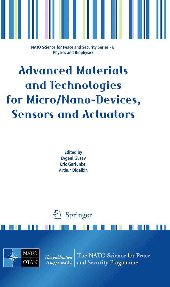
A NATO Advanced Research Workshop (ARW) entitled “Advanced Materials and Technologies for Micro/Nano Devices, Sensors and Actuators” was held in St. Petersburg, Russia, from June 29 to July 2, 2009. The main goal of the Workshop was to examine (at a fundamental level) the very complex scientific issues that pertain to the use of micro- and nano-electromechanical systems (MEMS and NEMS), devices and technologies in next generation commercial and defen- related applications. Micro- and nano-electromechanical systems represent rather broad and diverse technological areas, such as optical systems (micromirrors, waveguides, optical sensors, integrated subsystems), life sciences and lab equipment (micropumps, membranes, lab-on-chip, membranes, microfluidics), sensors (bio-sensors, chemical sensors, gas-phase sensors, sensors integrated with electronics) and RF applications for signal transmission (variable capacitors, tunable filters and antennas, switches, resonators). From a scientific viewpoint, this is a very multi-disciplinary field, including micro- and nano-mechanics (such as stresses in structural materials), electronic effects (e. g. charge transfer), general electrostatics, materials science, surface chemistry, interface science, (nano)tribology, and optics. It is obvious that in order to overcome the problems surrounding next-generation MEMS/NEMS devices and applications it is necessary to tackle them from different angles: theoreticians need to speak with mechanical engineers, and device engineers and modelers to listen to surface physicists. It was therefore one of the main objectives of the workshop to bring together a multidisciplinary team of distinguished researchers.
Häftad, Engelska, 2010
2 158 kr
Skickas inom 10-15 vardagar
A NATO Advanced Research Workshop (ARW) entitled “Advanced Materials and Technologies for Micro/Nano Devices, Sensors and Actuators” was held in St. Petersburg, Russia, from June 29 to July 2, 2009. The main goal of the Workshop was to examine (at a fundamental level) the very complex scientific issues that pertain to the use of micro- and nano-electromechanical systems (MEMS and NEMS), devices and technologies in next generation commercial and defen- related applications. Micro- and nano-electromechanical systems represent rather broad and diverse technological areas, such as optical systems (micromirrors, waveguides, optical sensors, integrated subsystems), life sciences and lab equipment (micropumps, membranes, lab-on-chip, membranes, microfluidics), sensors (bio-sensors, chemical sensors, gas-phase sensors, sensors integrated with electronics) and RF applications for signal transmission (variable capacitors, tunable filters and antennas, switches, resonators). From a scientific viewpoint, this is a very multi-disciplinary field, including micro- and nano-mechanics (such as stresses in structural materials), electronic effects (e. g. charge transfer), general electrostatics, materials science, surface chemistry, interface science, (nano)tribology, and optics. It is obvious that in order to overcome the problems surrounding next-generation MEMS/NEMS devices and applications it is necessary to tackle them from different angles: theoreticians need to speak with mechanical engineers, and device engineers and modelers to listen to surface physicists. It was therefore one of the main objectives of the workshop to bring together a multidisciplinary team of distinguished researchers.
E-bok
PDF, Engelska, 20102 840 kr
Läs direkt efter köp
A NATO Advanced Research Workshop (ARW) entitled “Advanced Materials and Technologies for Micro/Nano Devices, Sensors and Actuators” was held in St. Petersburg, Russia, from June 29 to July 2, 2009. The main goal of the Workshop was to examine (at a fundamental level) the very complex scientific issues that pertain to the use of micro- and nano-electromechanical systems (MEMS and NEMS), devices and technologies in next generation commercial and defen- related applications. Micro- and nano-electromechanical systems represent rather broad and diverse technological areas, such as optical systems (micromirrors, waveguides, optical sensors, integrated subsystems), life sciences and lab equipment (micropumps, membranes, lab-on-chip, membranes, microfluidics), sensors (bio-sensors, chemical sensors, gas-phase sensors, sensors integrated with electronics) and RF applications for signal transmission (variable capacitors, tunable filters and antennas, switches, resonators). From a scientific viewpoint, this is a very multi-disciplinary field, including micro- and nano-mechanics (such as stresses in structural materials), electronic effects (e. g. charge transfer), general electrostatics, materials science, surface chemistry, interface science, (nano)tribology, and optics. It is obvious that in order to overcome the problems surrounding next-generation MEMS/NEMS devices and applications it is necessary to tackle them from different angles: theoreticians need to speak with mechanical engineers, and device engineers and modelers to listen to surface physicists. It was therefore one of the main objectives of the workshop to bring together a multidisciplinary team of distinguished researchers.
E-bok
PDF, Engelska, 20122 049 kr
Läs direkt efter köp
An extrapolation of ULSI scaling trends indicates that minimum feature sizes below 0.1 mu and gate thicknesses of <3 nm will be required in the near future. Given the importance of ultrathin gate dielectrics, well-focused basic scientific research and aggressive development programs must continue on the silicon oxide, oxynitride, and high K materials on silicon systems, especially in the critical, ultrathin 1-3 nm regime. The main thrust of the present book is a review, at the nano and atomic scale, the complex scientific issues related to the use of ultrathin dielectrics in next-generation Si-based devices. The contributing authors are leading scientists, drawn from academic, industrial and government laboratories throughout the world, and representing such backgrounds as basic and applied physics, chemistry, electrical engineering, surface science, and materials science. Audience: Both expert scientists and engineers who wish to keep up with cutting edge research, and new students who wish to learn more about the exciting basic research issues relevant to next-generation device technology.