• Fri frakt över 249 kr
  • •
  • Snabba leveranser
  • •
  • Billiga böcker
Kundservice

Du är på sajten för privatpersoner.

Företag, bibliotek eller offentlig verksamhet?

Du handlar på classic.bokus.com, där alla dina funktioner finns intakta.
Till classic.bokus.com
Bokus logotyp. Gå till startsidan.
  • Erbjudanden
  • Nyheter
  • Student
  • Topplistor
  • Barn & ungdom
  • Bokus Play
  • E-böcker
  • Pocketböcker
  • Spel & pussel

10% rabatt på allt med kod: NYSTART10 →

Sidfot

Mina sidor

    Hjälp

    • Kundservice
    • Vanliga frågor och svar
    • Frakt och leverans
    • Retur vid ångerrätt
    • Reklamera vara
    • Betalning
    • Köpvillkor
    • Allmänna villkor
    • Information om webbplatsens tillgänglighet

    Om Bokus

    • Om oss
    • Pressrum
    • För studenter
    • För företag
    • För bibliotek och offentlig verksamhet
    • För leverantörer
    • Hållbarhet

    Populärt

    • Aktuella erbjudanden
    • Presentkort
    • Studentlitteratur
    • Nya böcker
    • Topplistor
    • Signerade böcker
    • Engelska böcker

    Inspiration

    • Boktips
    • BookTok
    • Populära bokserier
    • Barnbokskaraktärer
    • Populära författare
    Logotyp för Bokus
    Följ oss på Facebook (extern länk)Följ oss på Instagram (extern länk)Följ oss på YouTube (extern länk)Följ oss på TikTok (extern länk)
    bokus @ CookiesAnpassa cookiesIntegritetspolicyKöpvillkor
    Till Citymail hemsida (extern länk)Till Budbee hemsida (extern länk)Till Postnord hemsida (extern länk)Till Schenker hemsida (extern länk)Till Early Bird hemsida (extern länk)Till Walleys hemsida (extern länk)
    1. Naturvetenskap och teknik
    2. Teknik och industri
    3. Maskinteknik och material

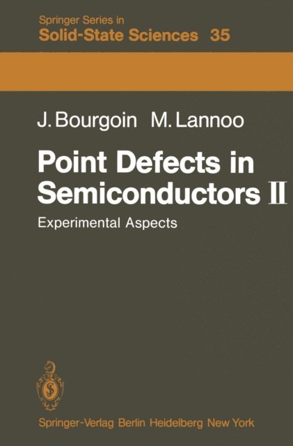
    Point Defects in Semiconductors II

    Experimental Aspects

    AvJ. Bourgoin

    Häftad, Engelska, 2011

    Del 35 i serien Springer Series in Solid-State Sciences

    1 086 kr

    Beställningsvara. Skickas inom 10-15 vardagar. Fri frakt över 249 kr.

    Fler format och utgåvor

    E-bok

    1 413 kr

    Beskrivning

    In introductory solid-state physics texts we are introduced to the concept of a perfect crystalline solid with every atom in its proper place. This is a convenient first step in developing the concept of electronic band struc­ ture, and from it deducing the general electronic and optical properties of crystalline solids. However, for the student who does not proceed further, such an idealization can be grossly misleading. A perfect crystal does not exist. There are always defects. It was recognized very early in the study of solids that these defects often have a profound effect on the real physical properties of a solid. As a result, a major part of scientific research in solid-state physics has,' from the early studies of "color centers" in alkali halides to the present vigorous investigations of deep levels in semiconductors, been devoted to the study of defects. We now know that in actual fact, most of the interest­ ing and important properties of solids-electrical, optical, mechanical- are determined not so much by the properties of the perfect crystal as by its im­ perfections.

    Produktinformation

    • Utgivningsdatum:2011-12-08
    • Mått:155 x 235 x 18 mm
    • Vikt:487 g
    • Format:Häftad
    • Språk:Engelska
    • Serie:Springer Series in Solid-State Sciences
    • Antal sidor:295
    • Förlag:Springer-Verlag Berlin and Heidelberg GmbH & Co. KG
    • ISBN:9783642818349

    Utforska kategorier

    • Maskinteknik och material inom Naturvetenskap och teknik

    Innehållsförteckning

    • 1. Introduction.- 2. Lattice Distortion and the Jahn-Teller Effect.- 2.1 The Electron-Phonon Interaction.- 2.2 Symmetry Considerations: The Stable Atomic Configurations.- 2.3 Coupled Electronic and Nuclear Motion: Vibronic States — Static and Dynamic Jahn-Teller Limits.- 2.4 The Vacancy in Silicon.- 3. Electron Paramagnetic Resonance.- 3.1 The Hamiltonian.- 3.2 Electronic Zeeman Interaction.- 3.3 Spin Orbit Coubling.- 3.4 Hyperfine Interaction.- 3.5 Nuclear Zeeman Interaction — Double Resonance.- 3.6 Spin-Spin Interaction. Fine Structure.- 3.7 EPR of Impurities and Vacancy — Impurity Pairs in Silicon.- 3.8 The Vacancy in Silicon.- 4. Optical Properties.- 4.1 Transition Probability.- 4.2 The Configuration Coordinate Diagram.- 4.3 Optical Line Shape and the Electron-Lattice Interaction.- 4.4 Optical Cross Section.- 4.5 An Example. The GR Absorption Band in Diamond.- 5. Electrical Properties.- 5.1 Carrier Distribution Between Bands and Defect Levels.- 5.2 Conduction in Case of Defect Interaction.- 5.3 Carrier Scattering.- 6. Carrier Emission and Recombination.- 6.1 Emission and Capture Rates.- 6.2 Experimental Observation of Emission Rates.- 6.3 Nonradiative Recombination Processes.- 6.4 Experimental Determination of Ionization Energies, Entropies and Cross Sections.- 6.5 Influence of the Electric Field on Emission Rates.- 7. Other Methods of Detection.- 7.1 Photoexcitation.- 7.2 Optical Detection of Paramagnetic Resonance.- 7.3 Direct Detection of Phonons.- 8. Defect Production by Irradiation.- 8.1 Interaction of Radiation with Solids.- 8.2 Defect Production.- 8.3 Defect Nature and Spatial Distribution.- 8.4 Experimental Determination of a Threshold Energy.- 8.5 Subthreshold Effects.- 9. Defect Annealing.- 9.1 Annealing Kinetics.- 9.2 Determination of the AnnealingParameters.- 9.3 Annealing of Defects Induced by Electron Irradiation.- References.