• Fri frakt över 249 kr
  • •
  • Snabba leveranser
  • •
  • Billiga böcker
Kundservice

Du är på sajten för privatpersoner.

Företag, bibliotek eller offentlig verksamhet?

Du handlar på classic.bokus.com, där alla dina funktioner finns intakta.
Till classic.bokus.com
Bokus logotyp. Gå till startsidan.
  • Erbjudanden
  • Nyheter
  • Student
  • Topplistor
  • Barn & ungdom
  • Bokus Play
  • E-böcker
  • Pocketböcker
  • Spel & pussel

10% rabatt på allt med kod: NYSTART10 →

Sidfot

Mina sidor

    Hjälp

    • Kundservice
    • Vanliga frågor och svar
    • Frakt och leverans
    • Retur vid ångerrätt
    • Reklamera vara
    • Betalning
    • Köpvillkor
    • Allmänna villkor
    • Information om webbplatsens tillgänglighet

    Om Bokus

    • Om oss
    • Pressrum
    • För studenter
    • För företag
    • För bibliotek och offentlig verksamhet
    • För leverantörer
    • Hållbarhet

    Populärt

    • Aktuella erbjudanden
    • Presentkort
    • Studentlitteratur
    • Nya böcker
    • Topplistor
    • Signerade böcker
    • Engelska böcker

    Inspiration

    • Boktips
    • BookTok
    • Populära bokserier
    • Barnbokskaraktärer
    • Populära författare
    Logotyp för Bokus
    Följ oss på Facebook (extern länk)Följ oss på Instagram (extern länk)Följ oss på YouTube (extern länk)Följ oss på TikTok (extern länk)
    bokus @ CookiesAnpassa cookiesIntegritetspolicyKöpvillkor
    Till Citymail hemsida (extern länk)Till Budbee hemsida (extern länk)Till Postnord hemsida (extern länk)Till Schenker hemsida (extern länk)Till Early Bird hemsida (extern länk)Till Walleys hemsida (extern länk)
    1. Naturvetenskap och teknik
    2. Teknik och industri
    3. Teknik: allmänt

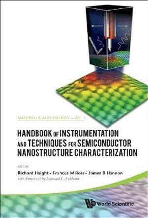
    HANDBOOK OF INSTRUMENTATION AND TECHNIQUES FOR SEMICONDUCTOR NANOSTRUCTURE CHARACTERIZATION (IN 2 VOLUMES)

    AvHAIGHT RICHARD,Richard Haight

    Inbunden, Engelska, 2011

    Del 2 i serien MATERIALS AND ENERGY

    5 481 kr

    Beställningsvara. Skickas inom 11-20 vardagar. Fri frakt över 249 kr.

    Beskrivning

    HighlightsFirst comprehensive handbook on instrumentation and techniques for semiconductor nanostructure characterizationMore than 900 references providing up-to-date information With over 260 illustrationsAs we delve more deeply into the physics and chemistry of functional materials and processes, we are inexorably driven to the nanoscale. And nowhere is the development of instrumentation and associated techniques more important to scientific progress than in the area of nanoscience. The dramatic expansion of efforts to peer into nanoscale materials and processes has made it critical to capture and summarize the cutting-edge instrumentation and techniques that have become indispensable for scientific investigation in this arena. This Handbook is a key resource developed for scientists, engineers and advanced graduate students in which eminent scientists present the forefront of instrumentation and techniques for the study of structural, optical and electronic properties of semiconductor nanostructures.

    Produktinformation

    • Utgivningsdatum:2011-12-01
    • Mått:158 x 235 x 44 mm
    • Vikt:1 362 g
    • Format:Inbunden
    • Språk:Engelska
    • Serie:MATERIALS AND ENERGY
    • Antal sidor:680
    • Förlag:World Scientific Publishing Co Pte Ltd
    • ISBN:9789814322805

    Utforska kategorier

    • Teknik: allmänt inom Naturvetenskap och teknik

    Innehållsförteckning

    • Atom Probe Tomography; Plasmon Dynamics of Nanostructured Surfaces; Scanning Tunneling Microscopy of Self Assembled III-V Nanostructures; Nanomembranes; Aberration Corrected Scanning Transmission Microscopy and Electron Energy Loss; Rayleigh Scattering from Carbon Nanotubes; Low Energy Electron Microscopy Studies of Nanostructured Semiconductor Surfaces; Scanning Probe Microscopy of GaN Based Structures; Time Domain Thermoreflectance for Thermal Characterization of Nanostructures; X-Ray Studies of Nanostructures; Single Nanowire Photoelectron Spectroscopy; Ultra-High Vacuum Transmission Electron Microscopy; Synthesis and Studies of Low-Dimensional Structures; Raman Spectroscopy of Carbon Nanotubes; Scanning Electron Microscopy for Characterization of Semiconducting Nanowires; X-Ray Diffraction for Stress Determination in Nanostructures.