• Fri frakt över 249 kr
  • •
  • Snabba leveranser
  • •
  • Billiga böcker
Kundservice

Du är på sajten för privatpersoner.

Företag, bibliotek eller offentlig verksamhet?

Du handlar på classic.bokus.com, där alla dina funktioner finns intakta.
Till classic.bokus.com
Bokus logotyp. Gå till startsidan.
  • Erbjudanden
  • Nyheter
  • Student
  • Topplistor
  • Barn & ungdom
  • Bokus Play
  • E-böcker
  • Pocketböcker
  • Spel & pussel

10% rabatt på allt med kod NYSTART10 →

Sidfot

Mina sidor

    Hjälp

    • Kundservice
    • Vanliga frågor och svar
    • Frakt och leverans
    • Retur vid ångerrätt
    • Reklamera vara
    • Betalning
    • Köpvillkor
    • Allmänna villkor
    • Information om webbplatsens tillgänglighet

    Om Bokus

    • Om oss
    • Pressrum
    • För studenter
    • För företag
    • För bibliotek och offentlig verksamhet
    • För leverantörer
    • Hållbarhet

    Populärt

    • Aktuella erbjudanden
    • Presentkort
    • Studentlitteratur
    • Nya böcker
    • Topplistor
    • Signerade böcker
    • Engelska böcker

    Inspiration

    • Boktips
    • BookTok
    • Populära bokserier
    • Barnbokskaraktärer
    • Populära författare
    Logotyp för Bokus
    Följ oss på Facebook (extern länk)Följ oss på Instagram (extern länk)Följ oss på YouTube (extern länk)Följ oss på TikTok (extern länk)
    bokus @ CookiesAnpassa cookiesIntegritetspolicyKöpvillkor
    Till Citymail hemsida (extern länk)Till Budbee hemsida (extern länk)Till Postnord hemsida (extern länk)Till Schenker hemsida (extern länk)Till Early Bird hemsida (extern länk)Till Walleys hemsida (extern länk)
    1. Naturvetenskap och teknik
    2. Teknik och industri
    3. Elektronik och kommunikationer

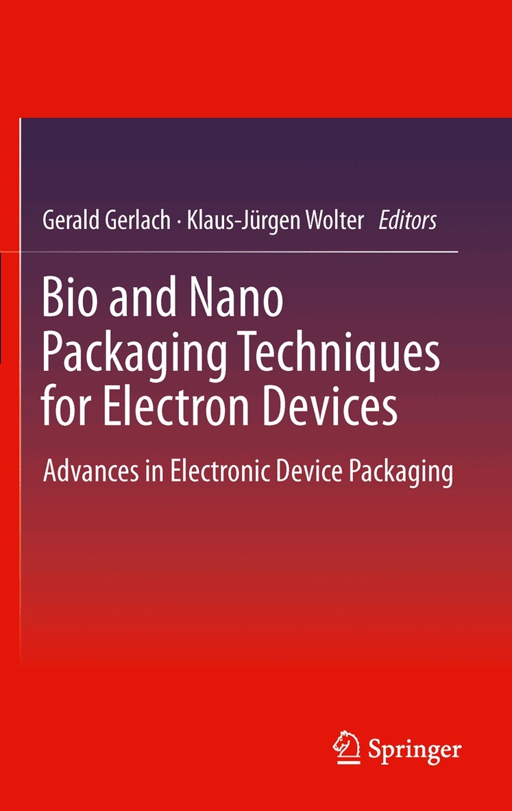
    Bio and Nano Packaging Techniques for Electron Devices

    Advances in Electronic Device Packaging

    AvGerald Gerlach,Klaus-Jürgen Wolter

    Inbunden, Engelska, 2012

    1 623 kr

    Beställningsvara. Skickas inom 10-15 vardagar. Fri frakt över 249 kr.

    Beskrivning

    This book discusses future trends and developments in electron device packaging and the opportunities of nano and bio techniques as future solutions. It describes the effect of nano-sized particles and cell-based approaches for packaging solutions with their diverse requirements. It offers a comprehensive overview of nano particles and nano composites and their application as packaging functions in electron devices. The importance and challenges of three-dimensional design and computer modeling in nano packaging is discussed; also ways for implementation are described. Solutions for unconventional packaging solutions for metallizations and functionalized surfaces as well as new packaging technologies with high potential for industrial applications are discussed. The book brings together a comprehensive overview of nano scale components and systems comprising electronic, mechanical and optical structures and serves as important reference for industrial and academic researchers.

    Produktinformation

    • Utgivningsdatum:2012-07-17
    • Mått:155 x 235 x 39 mm
    • Vikt:1 115 g
    • Format:Inbunden
    • Språk:Engelska
    • Antal sidor:628
    • Upplaga:2012
    • Förlag:Springer-Verlag Berlin and Heidelberg GmbH & Co. KG
    • ISBN:9783642285219

    Utforska kategorier

    • Elektronik och kommunikationer inom Naturvetenskap och teknik
    • Teknik: allmänt inom Naturvetenskap och teknik
    • Maskinteknik och material inom Naturvetenskap och teknik

    Mer om författaren

    Prof. Dr.-Ing. habil. Gerald Gerlach: 1983, 1987 Diploma and doctoral degree in EE from Technische Universitat Dresden, Germany, respectively R&D engineer in measuring devices industry. Since 1993 Professor for Microtechnology, since 1996 Professor for Solid State Electronics in EE department of TU Dresden. 2001/02 Visiting professor at UCLA. Since 2002 Member of the Executive of VDE (German Association of Engineers in Electrical Engineering, Electronics, Information Technology). Since 2007 Chairperson of the German Society for Measurement and Automatic Control (GMA). Since 1996 Conference Chairman of the biannually organised International Conference "Infrared Sensors and Systems IRS2" in Nuremberg (in conjunction with the world's largest sensor exhibition "Sensor+Test"). 2008 General Chairman of the Eurosensors XXII Conference, Dresden. Author and Co-author of some 280 scientific journal and international conference papers, holds more than 40 patents.Prof. Dr.-Ing. habil. Klaus-Juergen Wolter: 1967-1973 Studies in Control Theory at the Technical University Kiev, Ukraine. 1983 Dissertation "Correlation method for vision systems in microelectronics assembly". 1987 University Teaching Qualification (Habilitation). 1989-1973 R&D position the microelectronics industry. 1989 Assistant professor at the Institute of Electronic Technology. 1992 Appointment as Chair of Procedure Technology of Electronics. 1998 - 1999 Sabbatical at Tessera, San Jose, CA, (Wafer-Level-Packaging). Since 2002 Director of the Centre of Microtechnical Manufacturing (ZuP) at TUD. Since 2003 Director of the Electronic Packaging Lab at Dresden University of Technology. Since 2006 Deputy Head at Fraunhofer Institute IZFP Dresden. Fields of research: Substrate technologies, Assembly technologies of devices, components, MEMS, Joining technologies, Reliability of electronic packages, Non-destructive test methods

    Innehållsförteckning

    • General Aspects.- 3D Modelling and Design for Nems.- Nanoparticles.- Nanopatterning.- Metallization.- Nano- and Bio-Functionalized Surfaces.- Biocompatible Packaging.- Thermal Management.- System-In-Package For Mems and Moems.